
URL: https://fe.desy.de/fec/projects/miscellaneous/flip_chip_bonding/@@siteview
Breadcrumb Navigation
Flip-Chip Bonding
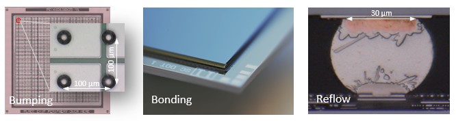
Project Goal:Installation & commissioning of in-house processes for fast prototyping & small-series productions. Project Status:Completed in 2022 Description:Flip-chip bonding is a key packaging technology to achieve smallest form factors and is nowadays a standard in microelectronics. The in-house bonding process comprises the full assembly chain utilizing a laser-assisted solder-ball bumper for micro bumping, a flip-chip bonder for accurate placement of the chips on top of each other, and a vacuum oven for the reflow of high-density array interconnects. This lead-free and flux-less chip-level bonding process utilizes SAC305-solder balls on pads and pillars with copper or nickel-(palladium)-gold surface finish. Chips which are already bumped can directly be bonded without any size limitations. The process is also applicable at low pressures and temperatures. Silicon-based semiconductor chips are preferred. |
|
1st Applications:
|